IRQuickScanTM Void Detection System
The IRQuickScanTM (IRQS) System utilizes a newly-developed, proprietary infrared detection scheme coupled with the powerful ClarityTM software platform to quickly characterize a variety of substrates for internal defects.
The IRQS System images any bonded wafer instantaneously, providing a detailed analysis that includes the location and classification of all defects associated with the bonding process. The BTBP Clarity SoftwareTM proprietary Artificial Intelligence engine, which is part of all BTBP Clarity products, locates all artifacts, classifies them, and produces a KLARF-like file, called the ClarityRF file.
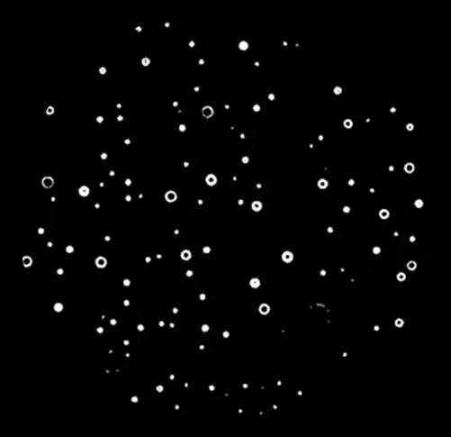
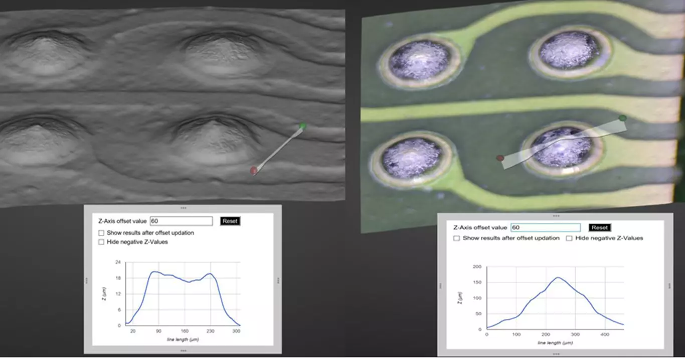
Here is an output from the IRQS System taken when imaging a bonded pair of silicon wafers with embedded metal pads, which exhibits voids and inclusions from the bonding process as well as the strain fields associated with bonding.

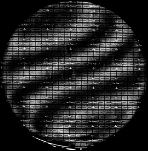
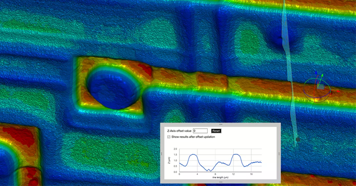
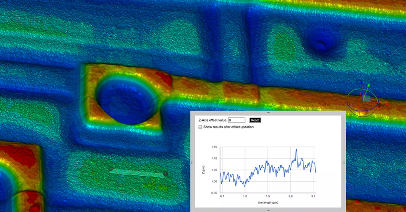
In addition, the IRQS System is able to provide the strain field signature on metalized production test wafers as shown here.
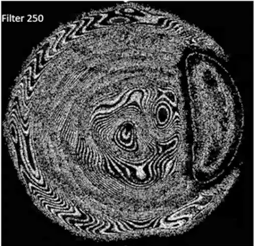
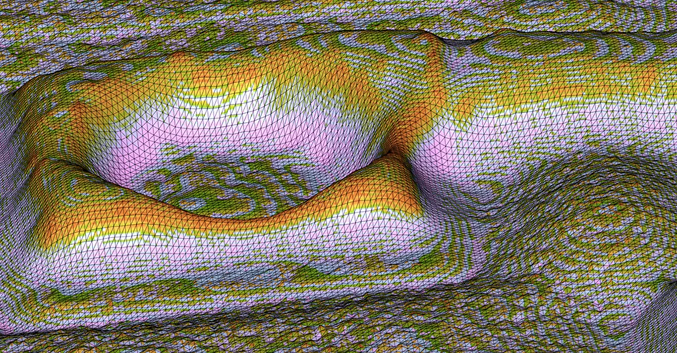
Of course the IRQS System is an ideal production tool for the SiC chip manufacturing environment since it allows detailed analysis of substrate crystal defects and associated strain fields as shown here.

The core value which drives the design of our systems is EASE OF USE. But we didn't stop there, in fact we started with our proprietary patented imaging technology and built a full system around it. Then we added our core expertise in Artificial Intelligence.
Introducing BTBP Clarity IRQS micro system through substrate inspection

Highlights
Out performs other systems in the market

Patented IRQS System
View voids clearly through IR
Multi Platform Software
Open platform to accommodate small to 300mm substrates
Automation customized for throughput & sample size
Clarity software for turnkey solution measurements to SEMI standards
Sub-micron for Voids & Strain Fields
Scanned with 17-bit depth in transmission scatter mode (1 part in 130,000)
100um pixel resolution
Standalone or automated
BOLTS configuration to SEMI standards for attachment to any EFFEM or process tool
Full wafer scan with 2-3mm edge exclusion
KLARF-like file output for location review capability
Turnkey recipe setup software
Lowest cost