Sub micron defect sensitivity
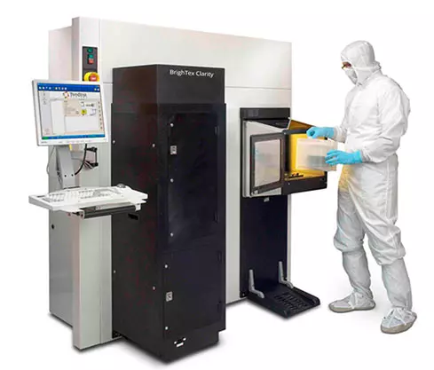
First system in the world to do wafer 3D & 2D analysis simultaneously
- Increase your yield with the most advanced A.I. in semiconductor metrology.
- BTBP's system detects and quantifies process defects.
- Wafer metrology is the key to process control and yield enhancement.

- Load & scan the wafer.
- Capture the full wafer for 2D and 3D analysis.
- Recipe setup and binning capability.
- Classify wafer defects and generate highest resolution 3D models for quantitative measurements.
- Detect & display defects like particles, scratches, missing patterns & bumps.
Highlights
DETECTING THE DEFECTS
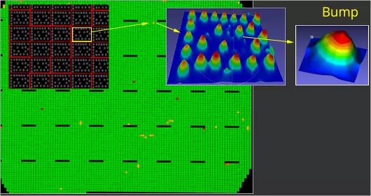
Bumps on the wafer:
- Identifying X, Y location(relative to notch), minimum height, maximum height, average height and diameter of the bump on a wafer.
- Information is saved in the industry standard KLARF format.

BINNING CAPABILITY
- Missing bumps can be identified.
- High quality imaging providing greater detail of intensities for detecting even floor variations & the height of bumps more accurately.
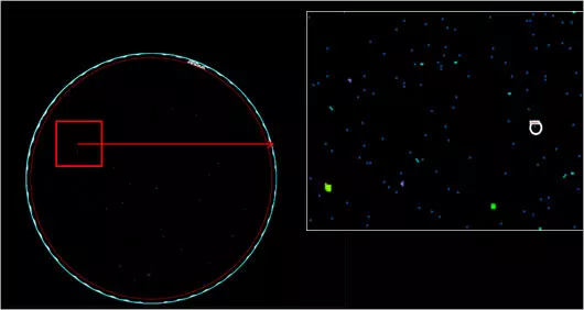
PARTICLES ON WAFER
- Features capable of detecting the presence of particles, residues, damaged wafers, wafer edges, hard & soft defects with their locations, count and size with high binning accuracy.
- 32 Bit High Dynamic Range Process of Scanning: Provides a wide range of intensities for detecting sub micron particles (0.25 microns) to very large particles (many millimeters) with a single scan for front and back of the wafer.
- Automatic classification of defects through our computer algorithm process of deep learning(A.I).
Application Features
Follows SEMI Standards for Job Handling
Recipe Management
User and Role Management
Access Control Based on Login
Defect/Particle Map in Standard Format
Charting Package for Professional Reporting
3D Viewer with Measurements
Die-to-Die Matching
2D and 3D Analysis
HDR Imaging
Edge Inspection
A.I. Available for Classifying Defects & Tagging defects
Signature Analysis
Automatic Notch detection
Brochure
